Transmission Electron Microscopy (TEM) is the best technique to view extremely thin and small objects (at the nanometer scale). This is achieved when the sample is shone with a high energy beam of electrons. The basic principles of operation are the same as transmitted light microscope but using electrons instead of light, and this allows for several order of magnitude better resolution, reaching, at the best conditions, features related to individual atoms. In addition, a TEM allows o obtain electron diffraction patterns allowing to access to structural information of the studied samples and to characterized its crystalline nature, or the absence of periodicity.
Main activities of our lab are the nanoscale characterization of materials focusing on: particle size and shape, phases characterization through diffraction and X-ray fluorescence, study of intergrowths and/or exsolutions, studies of defects and interfaces on both natural and synthetic samples.
Contacts
Equipment
The laboratory is equipped with
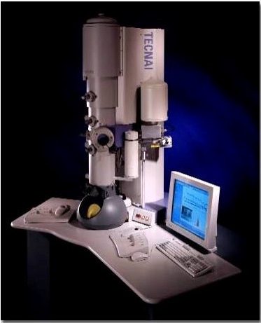
FEI Tecnai F20 Field Emission Gun (FEG) microscope, working at accelerating voltage of 200 kV.
A S-Twin system lens guarantees a point resolution of 0.24 nm, and an energy dispersive X-ray spectrometer (EDS) with ultrathin window allows for chemical characterization at the nanoscale.
The Transmission Electron Microscopy Laboratory is part of the UNITECH COSPECT - Comprehensive Substances characterization via advanced sPECTtroscopy (https://unitech.unimi.it/)
Responsabile Tecnico: Enrico Caneva
FEI Tecnai G2 F20
Main specifications
The FEI Tecnai F20 is a Field Emission Gun (FEG) transmission electron microscope.
The accelerating voltage is 200 kV.
The microscope is equipped with a S-Twin lens that gives a point resolution of 0.24 nm.
An energy dispersive X-ray spectrometer (EDS) with ultrathin window is present.
The imaging system is composed by one tv rate 626 Gatan and one slow scan 794 Gatan CCD cameras.
All the detectors are enbedded in the control unit of the microscope.
The sample holder is double tilt.
Thank to the FEG gun very small probes (<0.3 nm) are avilable.
Point resolution (nm) 0.24
Line resolution (nm) 0.1
Information limit (nm) 0.15
Cs objective (mm) 1.2
Cc objective (mm) 1.2
Focal length (mm) 1.7
Minimum focus step (nm) 1.8
Maximum eucentric tilt ± 40º
TEM magnification 25x – 1030 kx
SA diffraction camera length (mm) 40 – 4300
Maximum diffraction half angle ± 12º
Activity
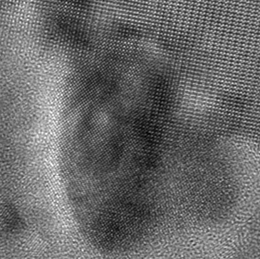
Electron Crystallography Structure analysis:
intergrowth, exsolution, interfaces Defect studies